

聯系電話:
 服務熱線:
服務熱線: 13917975482
服務熱線: 


| 品牌 | 其他品牌 | 價格區間 | 面議 |
|---|---|---|---|
| 儀器種類 | 微流控芯片系統 | 應用領域 | 電子/電池 |
| Nisene等離子芯片開封機 | PlasmaEtch |
當今世界越來越關注生態友好,半導體生產工藝的持續改進則進一步導致了集成電路內部組件尺寸越來越小,也變得越來越靈敏和脆弱。由此導致了芯片失效分析的一個特定挑戰:如何將樣品封裝去除卻不會導致功能失效? Nisene公司xin一代的芯片開封系統為半導體生產制造技術和失效分析之間的鴻溝搭建了一座橋梁:等離子芯片開封機—PlasmaEtch Nisene科技集團有限公司從事集成電路失效分析的自動開封裝置研發超過40年,擁有多項電化學及微波等離子開封機技術的專li。

The PlasmaEtch decapsulation system is a revolutionary patent-pending gas-based semiconductor etching system. Employing a never-before-seen application of microwaved gases inciting chemical radicals for isotropic etching, the PlasmaEtch is the greenest and most cost-effective etching solution available. The PlasmaEtch can etch most sample sizes, encapsulant types, and wire bond types. Whether it’s a more traditional gold wire sample, or if the sample features copper or silver wires, the PlasmaEtch delivers a safe and reliable etch.
PlasmaEtch創新點:
Afterburner Downstream Focused Plasma Etching(延時激發下行聚焦離子蝕刻)
Mass Flow Controlling for All Gases(所有氣體流量可控)
No Microwave Radiation Exposure to Samples During Etch Process(無微波輻射)
Low Temperature Etching(低溫蝕刻)
Isotropic Etching(等向性蝕刻)
Unlike typical and less sophisticated plasma decap systems that take many hours or even days to get to the surface of the die, the PlasmaEtch can clear the encapsulant of most package types and reveal the complete die surface and wire sweep in a matter of a couple hours. Chemical-free decapsulation has never been so effective.
主要特色(Highlights):
Highly Customizable Etch Recipes(高度可定制的蝕刻配方)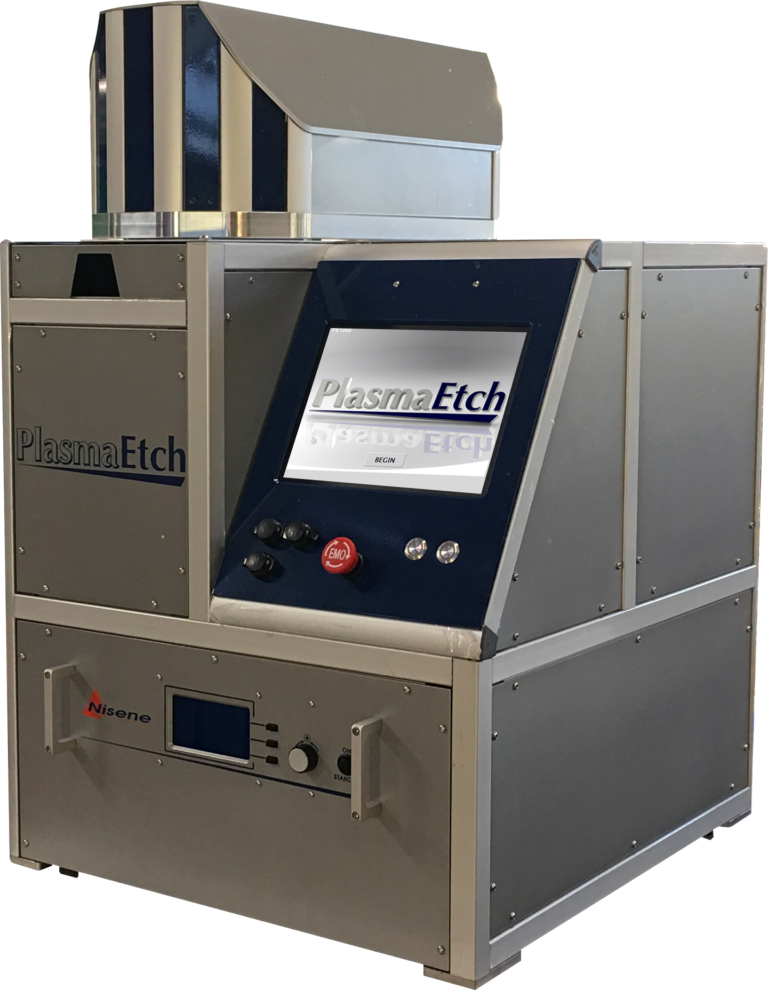
Etches a Wide Variety of Package Types(可蝕刻各種各樣的封裝類型)
Completely Chemical-free Decap(*非化學方式蝕刻)
Eco-friendly(生態友好環保)
Touchscreen Interface(觸控屏)
PC/Windows-based GUI(基于PC / Windows的GUI)
The Only Solution for Silver Wires(銀線的唯1解決方案)
Etches Samples with All Wire Types(可蝕刻所有引線類型的樣品)
Small Footprint Suited for Tabletop(桌上型緊湊尺寸機柜)

